
Computer-Aided Design, Analog & Digital VLSI Design
Faculty and Technical Support
- Faculty Coordinator: Dr. Devarshi Shukla (Assistant Professor)
- Technical Assistant: Mr. Sandeep Yadav
- Academic utilisation: Students of the 2nd, 3rd and 4th years.
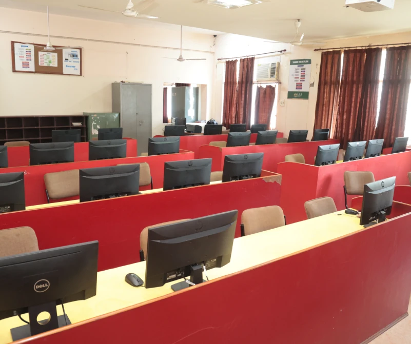
Established in the academic year 2016–2017, the CAD Design Lab at GLA University, Mathura, is a specialised teaching, design and research facility for analog and digital integrated-circuit design and digital hardware development. Using the available Cadence design environment and Xilinx FPGA tools, students can work through design specification, schematic or RTL entry, simulation, verification, synthesis, implementation and performance evaluation. Where the installed tools, process design kits (PDKs), technology files, verification decks and licence entitlements permit, the lab can also support custom IC layout verification and GDSII stream-out. The facility supports curriculum laboratories, mini- and major projects, faculty-guided research, skill-development workshops and project-based learning.
Objectives
- Develop practical skills in electronic design automation (EDA) for analog, digital and, where supported, mixed-signal IC design.
- Help students translate design specifications into schematics, HDL descriptions, testbenches and implementation constraints.
- Build competency in simulation, verification, synthesis, timing analysis, physical implementation and design-report interpretation.
- Introduce full-custom analog design and semi-custom / RTL-based digital design workflows.
- Support FPGA-based prototyping and hardware validation using supported Xilinx devices and boards.
- Promote design-oriented mini-projects, capstone projects, comparative design studies and faculty-guided research.
- Develop evidence-based problem solving, technical communication, teamwork, professional documentation and continuous improvement.
Major Tools and Design Activities
- Analog full-custom design: circuit specification, hand analysis, schematic capture, operating-point analysis, DC/AC/transient simulation, noise and corner analysis where supported, and design optimisation.
- Analog layout and physical verification: layout implementation, matching and symmetry practices where relevant, design-rule checking (DRC), layout-versus-schematic (LVS), parasitic-aware evaluation and GDSII stream-out where the configured flow supports them.
- Digital semi-custom design: architecture definition, Verilog/SystemVerilog or other supported HDL coding, testbench development, functional simulation, RTL synthesis, timing constraints and report analysis.
- ASIC-oriented physical design, where the required licensed environment is installed: floorplanning, power planning, placement, clock-tree synthesis, routing, timing closure and physical verification.
- Xilinx FPGA design: synthesis, technology mapping, placement and routing, timing analysis, bitstream generation and testing on supported devices or boards.
- Digital hardware prototyping: combinational and sequential logic, finite-state machines, counters, arithmetic units, controllers, datapaths, reusable IP, interfaces and selected DSP or hardware-accelerator blocks where hardware permits.
- Mixed-signal and cross-domain learning: analog/digital interfaces, comparator-based systems, clocking blocks and data-converter concepts where suitable tools and models are available.
- Verification and optimisation: systematic test plans, waveform/debug analysis, interpretation of DRC/LVS and timing reports, iterative improvement and documentation of whether requirements are met.
Academic and Research Activities
- Curriculum-based practicals related to Analog Electronics, Digital Electronics, Analog VLSI Design, Digital VLSI Design and HDL/FPGA Design, as applicable to the approved curriculum.
- Mini-projects and capstone projects involving specification, design, simulation, verification, implementation and technical reporting.
- Faculty-guided research in low-power circuits, analog front ends, amplifier topologies, memory and compute structures, digital accelerators, FPGA implementation and design optimisation, subject to available tools and expertise.
- Comparative design studies evaluating parameters such as gain, bandwidth, noise, power, area, delay, timing margin and resource utilisation.
- Skill-development workshops on EDA workflows, schematic capture, circuit simulation, HDL coding, testbench development, synthesis, timing analysis, layout and FPGA prototyping.
- Student innovation projects for communication, sensing, instrumentation, automation and edge-processing applications compatible with the available resources.
- Technical documentation and dissemination through design notebooks, reports, posters, presentations, project demonstrations and technical papers where appropriate.
Lab Utilisation and Research Activities
| Activity | Utilisation / Achievement |
|---|---|
| Ph.D. research | 3 ongoing and 7 completed Ph.D. research activities. |
| Undergraduate (UG) projects | 40 UG projects, including third-year and final-year projects. |
| Faculty Development Programs (FDPs) | 5 Faculty Development Programs. |
| Workshops | 5 workshops. |
| Software / Resource | Availability | Primary use |
|---|---|---|
| Cadence | 30-user Cadence Research Bundle | Analog and digital IC design, schematic capture, simulation, layout and verification where supported. |
| Xilinx | 25-user licence bundle | RTL-based digital design, synthesis, FPGA implementation and hardware validation on supported devices. |
| Lab infrastructure | 51 workstations; AB2-211 and AB2-212 | Design entry, simulation, implementation, project documentation and result analysis. |
| Technology / hardware | gpdk 45 nm, 90 nm and 180 nm; PYNQ-Z2 board | Technology-based design exercises and FPGA prototyping, subject to tool, model and licence availability. |
Expected Outcomes
- Students will be able to convert a design brief into measurable requirements and select an appropriate analog, digital or FPGA-based design approach.
- Students will gain practical familiarity with the installed EDA tools and learn to manage schematics, HDL source files, testbenches, constraints, simulation setups and implementation projects.
- Students will develop and verify analog circuits, digital RTL modules or FPGA prototypes against defined functional requirements.
- Students will interpret simulation waveforms and implementation reports, identify faults, and present evidence of functional correctness.
- Students will evaluate relevant design metrics such as gain, bandwidth, noise, power, area, delay, timing margin and FPGA resource utilisation, as applicable.
- Students will compare design alternatives, justify engineering choices using measured or simulated results, and document the effect of design iterations.
- Students will understand the purpose of layout, parasitic effects, DRC, LVS and GDSII output in an IC design flow.
- Students will strengthen teamwork, technical communication, project management, professional documentation and independent learning skills.
- The lab can support improved project quality, faculty-guided research, practical tool readiness and evidence for outcome-based education and NBA assessment, with impact demonstrated through actual student work and assessment records.
Illustrative Projects
- Analog amplifier or comparator design and characterisation.
- Analog layout implementation with available DRC/LVS checks.
- Digital finite-state machine, arithmetic unit, counter or controller with testbench and synthesis reports.
- FPGA-based digital system validated against simulation results.
- Timing and resource optimisation study using implementation reports.
- ASIC-oriented implementation and GDSII study where the required tools, libraries and licences are available.
- Integrated mini-project documenting requirements, architecture, implementation, verification, results and limitations.
 Virtual Tour
 B.Tech Programs
UG Programs
Lateral Entry
M.Tech Programs
PG Programs
Doctoral Programs
Diploma Programs
Admissions Helpline

-

-

-

-

17km Stone, NH-19, Mathura-Delhi Road, P.O.
Chaumuhan, Mathura-281 406, (U.P.) INDIA